
Facilities
Facilities
The department of materials engineering sets up many professional labs, either for general educational purpose or for professional research. The equipment includes high-resolution transmission electron microscope (HR-TEM), field emission scanning electron microscope (FE-SEM), atomic force microscope (AFM), X-ray diffraction (XRD), UV-Vis Spectroscopy, Raman spectroscopy, FTIR spectroscopy, nano indenter, thermal analysis (DSC, TGA), etc., as well as many thin film and coating processing facilities, such as high power impulse magnetron sputtering (HIPIMS).
| Lab | Name of labs |
|
Ultrahigh Resolution Scanning Electron Microscope Lab |
|
|
TEM Lab |
|
|
Surface Treatment Lab |
|
|
Fuel Cell Materials Lab |
|
|
X-Ray Diffraction Lab |
|
|
SEM Lab |
|
|
Optoelectronic Polymer Lab |
|
|
Plasma & Functional Thin Films Lab |
|
|
Ceramic Integrated Circuit Lab |
|
|
Nano Surface Analysis Lab |
|
|
Characterization of Optoelectronic Properties Lab |
|
|
Physical Vapor Deposition Lab |
|
|
Advance Carbon Nano-materials and Renewable Energy Lab |
|
|
Nanotechnologies for Information Storage Lab |
|
|
Organic Optoelectronics and Nano Energy Lab |
|
|
Semiconductor Materials Lab |
|
|
Electronic Materials Lab |
|
|
Nanostructure Lab |
|
| Thin Film Procedural Hydrogen Lab | |
| Advanced Nano Materials and Processes Lab | |
| NanoScience and BioInterface Lab. | |
| Integrated Nanomaterials and Bioelectronics Lab | |
| Electron Microscope Lab | |
|
Simulation for Materials and Processes Lab |
|
| Equipment |
Piezoelectric Ink-Jet Printer |
|
Atomic Force Microscopy (AFM) |
|
|
Differential Scanning Calorimeter (DSC) |
|
|
Thermogravimetric Analyzer (TGA) |
|
|
Magnetron Sputtering |
|
|
Hall Effect Measurement System |
|
|
Fluorescence Spectrometers |
|
|
Field Emission Scanning Electron Microscope (FE-SEM) |
|
|
Scanning Electron Microscope (SEM) |
|
|
Energy Disperse Spectroscopy (EDS) |
|
|
X-Ray Diffractive (XRD) |
|
|
4-Point Probe |
|
|
Nano Indenter |
|
|
UV/VIS Spectrophotometer |
|
|
Thermal Evaporation |
|
|
Ellipsometer |
|
|
Rapid Thermal Annealing (RTA) Oven |
|
|
Semiconductor Parameter Analyzer |
|
|
Raman scattering spectrometer |
|
|
AC Impedance Spectrometer |
|
|
Transmission Electron Microscopy(TEM) |
|
|
Precision Ion Polishing System (PIPS) |
|
|
Monochromatic Incident Photon-to-electron Conversion Efficiency (IPCE) |
|
|
Thermal Evaporator for Organic Electronic Materials |
|
|
High Power Impulse Magnetron Sputtering (HIPIMS) |
|
|
Profilometer |
|
(1)High Resolution FE-SEM (JEM-6701)
|
HighResolutionFE-SEM(JEM-6701).png) |
|
(2)High Resolution TEM(JEM-2100)
|
HighResolutionTEM(JEM-2100).png) |
|
(3)Nanoindenter (Hysitron TI 900 TriboIndenter)
|
Nanoindenter(HysitronTI900TriboIndenter).png) |
|
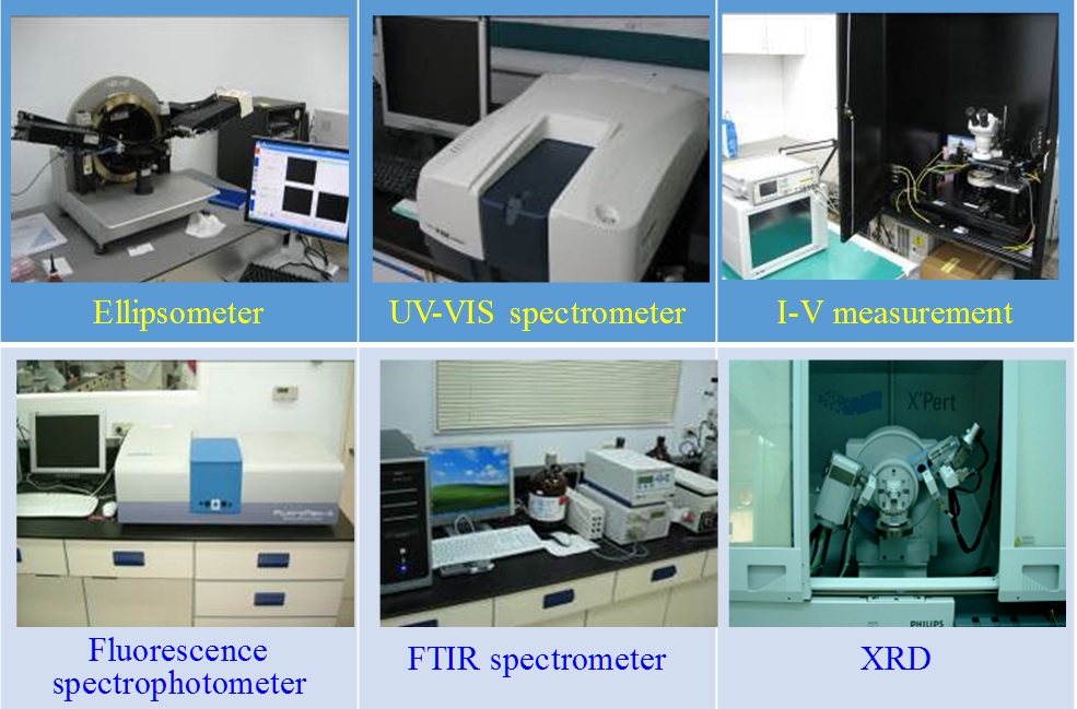
(4)Ellipsometer, UV-Vis Spectroscopy, I-V measurement,
Fluorescence spectrophotometer, FTIR Spectrometer, X-ray Diffraction (XRD)
|
 |
|
(5)Atomic Force Microscope (AFM), TEM Ion Miller, RTA,
Raman Spectroscopy, SEM/EDS, Glove Box
|
AtomicForceMicroscope(AFM),TEMIonMiller,RTA,RamanSpectroscopy,SEMEDS,GloveBox.png) |
|
(6)Thin film and coating processing facilitie
|
Thinfilmandcoatingprocessingfacilities.png) |
|
(7)High Power Impulse Magnetron Sputtering (HIPIMS)
|
HighPowerImpulseMagnetronSputtering(HIPIMS).png) |